3.2 KiB
Specifications
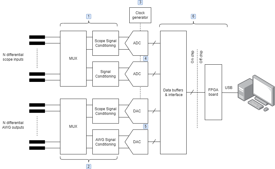
The purpose of this page is to seed some ideas on what the “lab bench on a chip” target design may look like. Further teamwork and thinking is required to turn this into a workable design that we can tape out toward the end of the year. Each participating team may choose to work on one or more of the six building blocks identified in the diagram below. The proposals submitted by each team (in the form of a Jupyter notebook) should describe in detail how you want to implement your chosen block(s), what the specifications will be, and in addition provide convincing calculations and simulation results. Layouts are not required at the proposal stage.

To our knowledge, there aren't any published prior-art designs that we can build on. However, we can draw some inspiration from a similar system that was designed for discrete circuits. The Analog Discovery 2 is a multifunction instrument that has all the functionality we are looking for (and more) and comes with detailed schematics. While this documentation provides a first-order idea on what we should build, the circuit design style will be somewhat different for on-chip circuitry. Additionally, it will be difficult to match all specifications within a reasonable area budget and given the 180 nm technology that we have at our disposal.
What follows below are initial thoughts and minimum specs for each one of our major system components. All teams are encouraged to exceed the minimum requirements and explore what is possible!
1. Scope MUX and signal conditioning
The oscilloscope design should have an input MUX that allows the macro's user to switch the ADC to a number of different test points within the DUT. It is desirable to have the MUX work for rail-to-rail inputs. The signal conditioning circuitry should have a small input capacitance and essentially "infinite" input resistance. On the output side, there must be significant drive strength to handle the high-speed ADCs and deal with their charge kickback (if applicable). A plus for signal conditioning block would be to include transimpedance stages for current measurements.
| Specification | Symbol | Baseline requirement | Comment |
|---|---|---|---|
| Scope input capacitance | Cin | <5pF | From each diff. input to ground |
| Number of differential input channels | N | >=8 | |
| Noise | Neq | <0.5 LSBrms | Contribution of the front-end to the ADC's sampled noise |
2. AWG MUX and signal conditioning
3. Clock generator
4. ADCs
5. DACs
6. Digital interface
One of the primary goals here is to enable a convenient USB interface to a host computer. Teams working on this aspect should design both the on- and off-chip digital circuitry. For the off-chip board, we can consider the lowest cost boards from Digilent. The USB UART provided here could be useful for establishing the communication.